- 您现在的位置:买卖IC网 > Sheet目录3880 > PIC12F683-I/MD (Microchip Technology)IC PIC MCU FLASH 2KX14 8DFN
2007 Microchip Technology Inc.
DS41211D-page 9
PIC12F683
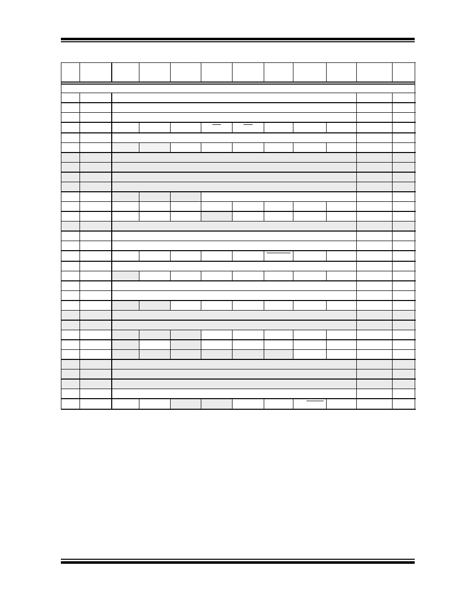
TABLE 3-1:
PIC12F683 SPECIAL REGISTERS SUMMARY BANK 0
Addr
Name
Bit 7
Bit 6
Bit 5
Bit 4
Bit 3
Bit 2
Bit 1
Bit 0
Value on
POR, BOR
Page
Bank 0
00h
INDF
Addressing this location uses contents of FSR to address data memory (not a physical register) xxxx xxxx 17, 90
01h
TMR0
Timer0 Module Register
xxxx xxxx
02h
PCL
Program Counter’s (PC) Least Significant Byte
0000 0000
03h
STATUS
IRP(1)
RP1(1)
RP0
TO
PD
ZDC
C
0001 1xxx
04h
FSR
Indirect Data Memory Address Pointer
xxxx xxxx
05h
GPIO
—
GP5
GP4
GP3
GP2
GP1
GP0
--xx xxxx
06h
—
Unimplemented
—
07h
—
Unimplemented
—
08h
—
Unimplemented
—
09h
—
Unimplemented
—
0Ah
PCLATH
—
Write Buffer for upper 5 bits of Program Counter
---0 0000
0Bh
INTCON
GIE
PEIE
T0IE
INTE
GPIE
T0IF
INTF
GPIF
0000 0000
0Ch
PIR1
EEIF
ADIF
CCP1IF
—
CMIF
OSFIF
TMR2IF
TMR1IF
000- 0000
0Dh
—
Unimplemented
—
0Eh
TMR1L
Holding Register for the Least Significant Byte of the 16-bit TMR1
xxxx xxxx
0Fh
TMR1H
Holding Register for the Most Significant Byte of the 16-bit TMR1
xxxx xxxx
10h
T1CON
T1GINV
TMR1GE
T1CKPS1 T1CKPS0 T1OSCEN T1SYNC
TMR1CS
11h
TMR2
Timer2 Module Register
0000 0000
12h
T2CON
—
TOUTPS3 TOUTPS2 TOUTPS1 TOUTPS0 TMR2ON
T2CKPS1
13h
CCPR1L
Capture/Compare/PWM Register 1 Low Byte
xxxx xxxx
14h
CCPR1H
Capture/Compare/PWM Register 1 High Byte
xxxx xxxx
15h
CCP1CON
—
DC1B1
DC1B0
CCP1M3
CCP1M2
CCP1M1
16h
—
Unimplemented
—
17h
—
Unimplemented
—
18h
WDTCON
—
WDTPS3
WDTPS2
WDTPS1
WDTPS0
19h
CMCON0
—COUT
—
CINV
CIS
CM2
CM1
CM0
-0-0 0000
1Ah
CMCON1
—
T1GSS
1Bh
—
Unimplemented
—
1Ch
—
Unimplemented
—
1Dh
—
Unimplemented
—
1Eh
ADRESH
Most Significant 8 bits of the left shifted A/D result or 2 bits of right shifted result
xxxx xxxx
1Fh
ADCON0
ADFM
VCFG
—
CHS1
CHS0
GO/DONE
ADON
00-- 0000
Legend:
– = unimplemented locations read as ‘0’, u = unchanged, x = unknown, q = value depends on condition,
shaded = unimplemented
Note
1:
IRP and RP1 bits are reserved, always maintain these bits clear.
发布紧急采购,3分钟左右您将得到回复。
相关PDF资料
XF2L-2125-1
CONN FPC 21POS 0.5MM SMT
XF2L-2035-1
CONN FPC 20POS 0.5MM SMT
PIC18F8621T-I/PT
IC PIC MCU FLASH 32KX16 80TQFP
XF2L-1835-1
CONN FPC 18POS 0.5MM SMT
XF2L-1535-1
CONN FPC 15POS 0.5MM SMT
PIC16LF767T-I/SO
IC PIC MCU FLASH 8KX14 28SOIC
XF2L-1335-1
CONN FPC 13POS 0.5MM SMT
XF2L-1325-1
CONN FPC 13POS 0.5MM SMT
相关代理商/技术参数
PIC12F683-I/MDQTP
制造商:MICROCHIP 制造商全称:Microchip Technology 功能描述:8-Pin Flash-Based, 8-Bit CMOS Microcontrollers with nanoWatt Technology
PIC12F683-I/MF
功能描述:8位微控制器 -MCU 3.5KB 128 RAM 6 I/O RoHS:否 制造商:Silicon Labs 核心:8051 处理器系列:C8051F39x 数据总线宽度:8 bit 最大时钟频率:50 MHz 程序存储器大小:16 KB 数据 RAM 大小:1 KB 片上 ADC:Yes 工作电源电压:1.8 V to 3.6 V 工作温度范围:- 40 C to + 105 C 封装 / 箱体:QFN-20 安装风格:SMD/SMT
PIC12F683-I/MF
制造商:Microchip Technology Inc 功能描述:8BIT FLASH MCU SMD 12F683 DFN-8
PIC12F683-I/MFQTP
制造商:MICROCHIP 制造商全称:Microchip Technology 功能描述:8-Pin Flash-Based, 8-Bit CMOS Microcontrollers with nanoWatt Technology
PIC12F683-I/P
功能描述:8位微控制器 -MCU 3.5KB 128 RAM 6 I/O RoHS:否 制造商:Silicon Labs 核心:8051 处理器系列:C8051F39x 数据总线宽度:8 bit 最大时钟频率:50 MHz 程序存储器大小:16 KB 数据 RAM 大小:1 KB 片上 ADC:Yes 工作电源电压:1.8 V to 3.6 V 工作温度范围:- 40 C to + 105 C 封装 / 箱体:QFN-20 安装风格:SMD/SMT
PIC12F683-I/P
制造商:Microchip Technology Inc 功能描述:IC 8BIT FLASH MCU 12F683 DIP8
PIC12F683-I/PQTP
制造商:MICROCHIP 制造商全称:Microchip Technology 功能描述:8-Pin Flash-Based, 8-Bit CMOS Microcontrollers with nanoWatt Technology
PIC12F683-I/SN
功能描述:8位微控制器 -MCU 3.5KB 128 RAM 6 I/O RoHS:否 制造商:Silicon Labs 核心:8051 处理器系列:C8051F39x 数据总线宽度:8 bit 最大时钟频率:50 MHz 程序存储器大小:16 KB 数据 RAM 大小:1 KB 片上 ADC:Yes 工作电源电压:1.8 V to 3.6 V 工作温度范围:- 40 C to + 105 C 封装 / 箱体:QFN-20 安装风格:SMD/SMT